Department of Physics
226 Physics Building
825 West Dickson Street
University of Arkansas
Fayetteville, AR 72701
P 479-575-2506
E-mail: physics@uark.edu
Paul Thibado Research Lab
Molecular Beam Epitaxy (MBE) Facility
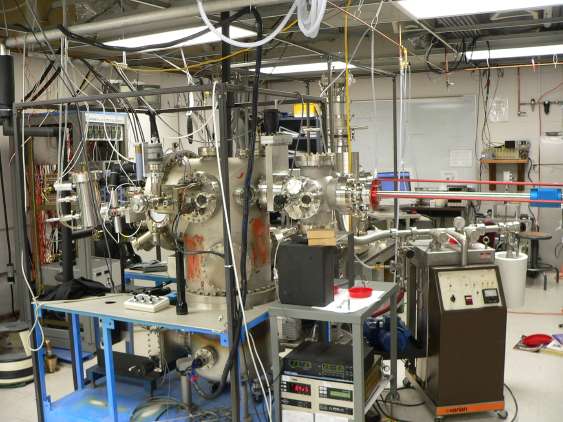
Using this facility we can prepare our own samples. We typically start with a commercially available GaAs wafer, introduce it into the MBE facility and deposit a thin film of GaMnAs to form a ferromagnetic semiconductor. The red bars on the right side of the picture allow us to put in the wafer and take out our sample without disturbing the vacuum. The electronics rack in the background behind the chamber allows us to control the temperature of the Ga, As, and Mn cells, and the temperature of the sample.
Low-Temperature Scanning Tunneling Microscope (LT-STM) Facility
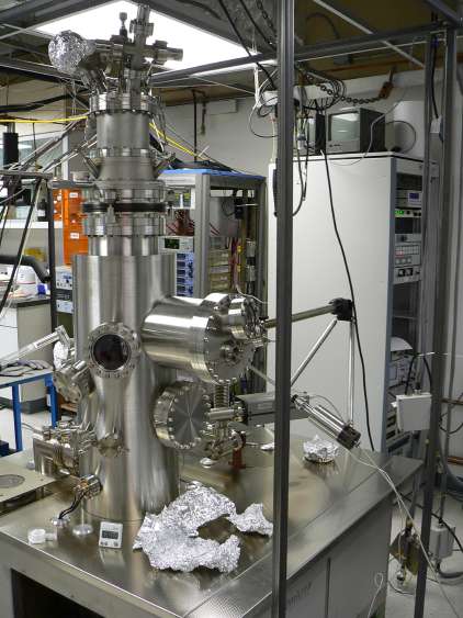 Using this facility we can take pictures of the surface of the GaAs samples we prepare
inside the MBE facility. The microscope can image individual atoms on the surface.
This facility is customized to have two microscopes that can image the sample simultaneously;
each with atomic resolution and each can image the same location on the sample. The
imaging is accomplished by injecting a small current into the sample. With two microscopes
we can inject a small current at one location and then detect that same current a
few nanometers away. This unique ability allows us to study how various properties
of the electron can change when it moves through a small man-made structure.
Using this facility we can take pictures of the surface of the GaAs samples we prepare
inside the MBE facility. The microscope can image individual atoms on the surface.
This facility is customized to have two microscopes that can image the sample simultaneously;
each with atomic resolution and each can image the same location on the sample. The
imaging is accomplished by injecting a small current into the sample. With two microscopes
we can inject a small current at one location and then detect that same current a
few nanometers away. This unique ability allows us to study how various properties
of the electron can change when it moves through a small man-made structure.